
HILLSBORO, Ore. — With millions of federal and state dollars going toward the semiconductor industry in Oregon's Silicon Forest, high-tech companies like Intel are preparing to make some big moves. The Story's Pat Dooris got a rare chance to go inside an Intel fabrication plant, or "fab," to find out more about what the tech giant is cooking up.
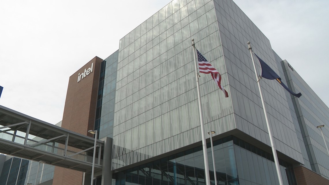
Intel's headquarters are in California, but the company's highest headcount is in Oregon. Its four campuses in Hillsboro take semiconductor chips from the imagination of engineers, through research and development and into early manufacturing and some mass production before the blueprint gets passed on to other Intel sites around the world.
The company reports that it has 22,000 employees in Oregon and supports another 100,000 jobs. It's spent $4 billion with Oregon-based suppliers and invested $59 billion in its Oregon plants over the years. It's one of the leading makers of semiconductors in the world, developing the chips that run many global data centers and PCs.
Engineers and developers at Intel are always working to push the boundaries of what's possible, leaning on Moore's Law — the idea that the number of transistors on a single chip will double every two years with a minimal increase in cost.
But over the last five years, Intel has had its ups and downs, demonstrated by the wavering value of its stock. It went from a high of $68 per share to more recently trading at $36 per share.
By investing $100 billion in American factories and innovation, the company hopes to turn that trend around. In late March, the company learned that it had secured $8.5 billion from the Biden administration, paired with another $11 billion in loans, with the goal of bringing chip manufacturing back to the U.S.
CEO Pat Gelsinger celebrated the news with President Joe Biden at a fab under construction in Arizona.
"Today is a victory for America's national economy — but also our national security," Gelsinger said. "It's a victory for American innovation."
Intel has said that these funds will be used to support fabs and research centers in Arizona, Ohio, New Mexico and Oregon.
Moore's vanguard
Around the beginning of this year, cargo planes flew into Seattle from a company called ASML in The Netherlands. They carried 250 crates spread throughout 43 freight containers, which were then loaded onto 20 semi-trucks for the trip south to Intel in Oregon. Dooris was there in January when the first pieces began arriving at Intel's Gordon Moore Park.
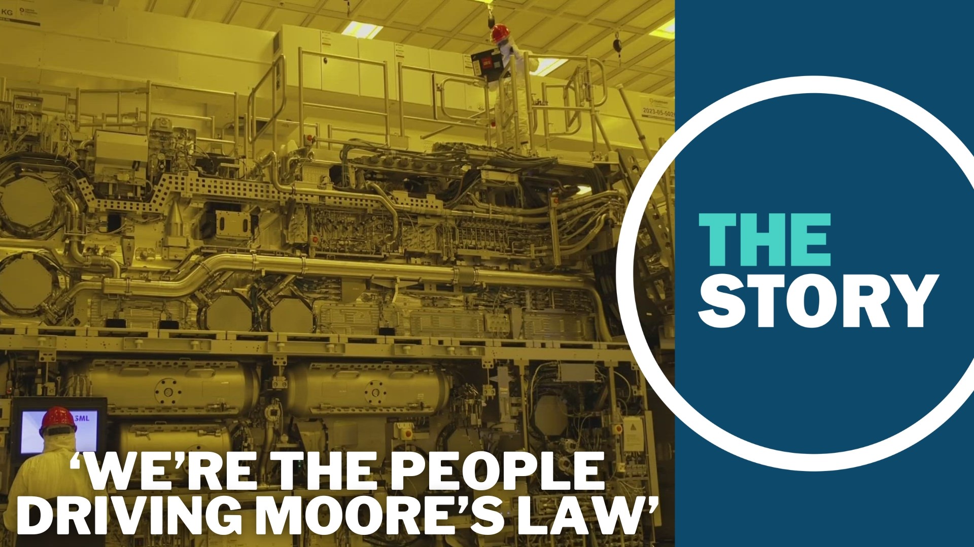
The machine assembled from these pieces shipped by ASML is called a High Numerical Aperture Extreme Ultraviolet tool, or High NA EUV. Right now, Intel is the only corporation in the world with one of these machines, which trade publications said cost around $380 million.

Ryan Russell was one of the many on hand for its arrival. He runs the group responsible for Intel's next generation fab process development.
"We are the people driving Moore's Law for Intel," he said.
And this machine is supposed to allow them to drive it further.
"When we make semiconductors, we start out with a piece of silicon and we put a pattern down on it," Russell explained. "Then, we develop that pattern into the silicon. Then we basically rinse and repeat that. So, it's a lot like building a skyscraper. We come in, you basically put down one floor, we develop it. Then you construct a second floor, you construct a third floor, all the way up. This machine is how we basically put down the pattern for what we're gonna make on that floor."
The High NA EUV machine will allow them to make the microscopic features on a chip even smaller than before, while still producing accurate results.
"It will make things smaller, but the second thing this tool brings to us is a lot more precision in where we put those items," Russell continued. "And that becomes very important. If I go back to the skyscraper analogy, when you build that first floor, you're gonna have an elevator shaft on it. When you put that second floor down, you not only — we're trying to make it smaller, but we need those elevators shafts to stack up on top of each other. If they're not lined up all the way through the building, you can't actually run an elevator car through it.
"So, this machine vastly improves the capability that we have to place that elevator shaft and to make sure that as we stack them up, they work."
Some microchips have up to a billion transistors on them now. This machine could push that number up even higher.
Absolutely fabricated
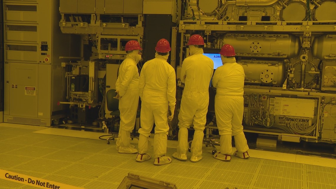
It took several weeks for teams of techs from ASML to assemble the High NA EUV machine, but by mid-April, it was largely in place and ready to go. That's when Dooris got a tour of the D1X Fab in Hillsboro.
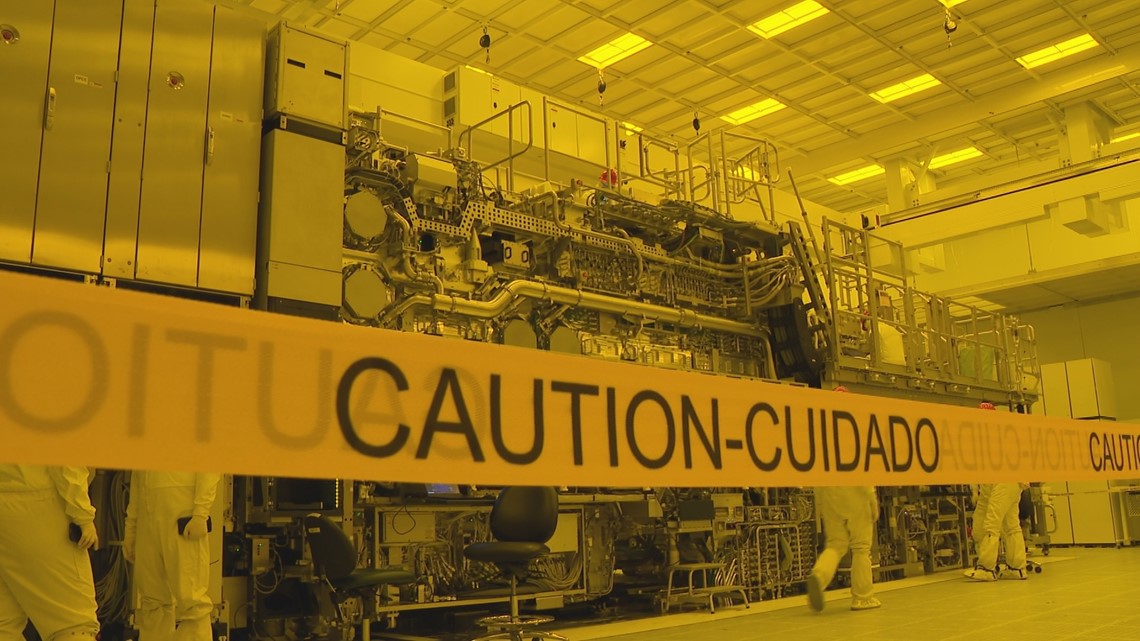
Before getting inside the clean room atmosphere, Dooris had to don a "bunny suit." It included a head cover, two layers of shoe covers, gloves, and a suit meant to keep all of his debris away from the merchandise. The machines used in these high-tech facilities are so precise, so fine-tuned that a human hair in the wrong place could ruin the product.

The fab at Gordon Moore is four football fields long and equally wide, filled with expensive machinery. Intel says that it costs about $10 billion to build and outfit a single fab like this one, requiring three years to complete.
When it comes to creating these silicon wafers, the machines do all the work. It's the job of human employees to monitor the machines.
Mary Huston joined Intel after her junior year of high school, 40 years ago. She used to walk 10 miles a day in the fab, but now an overhead system carries the silicon wafers, making the trip unnecessary.
"People think that, you know, automation is taking over our jobs," Huston said. "It's really not. We're just focused on other things now."
The High NA EUV tool is massive in its own right, about the size of a tennis court. It has 100,000 parts and weighs nearly 200 tons. The magic happens within it, in parts hidden from human eyes.
Moore's Law was coined by Intel co-founder Gordon Moore, the namesake for this campus. And for his law to remain remotely true — that the number of transistors squeezed onto a single chip will double about every two years — the transistors need to become microscopic.
A machine of the future
To print a pattern for the transistors and other components, chip companies use lithography machines. They project circuit patterns onto a special coating atop the silicon wafers. Over the years, they've made the wavelength of light short and shorter on lithography, allowing them to print features for ever smaller transistors.
But to make transistors even tinier still, the semiconductor industry needs lithography machines with even shorter wavelengths, the kinds that don't naturally exist. Extreme ultraviolet light is artificial and must be produced, which is part of what the High NA EUV tool accomplishes.
Because it's so massive, the machine needs three floors in the fab. It has a powerful laser that sits one floor below, with a beam 15 times the power of lasers used to cut steel. A beam transport sends the laser up a floor to the machine, where a generator fires tiny drops of tin in a vacuum — each drop a third as thick as a human hair.

This laser, flashing 50,000 times a second, hits the tin droplet and vaporizes it into a plasma, which in turn releases light in the extreme ultraviolet range. A collector mirror then catches the EUV light and shoots it to a scanner, where it bounces off extremely precise mirrors that shape the light into slits — creating the miniscule patterns of transistors and connectors on a silicon wafer.
And the kind of chips it will help produce don't even exist as yet. Intel said it could be two or three years before it even begins making chips with this machine. They'll be called "14A" chips, heralded among the most advanced in the world and envisioned for use in artificial intelligence and much more.
At Intel, people are very excited about the machine, these future chips, and what they mean for the company — and for Oregon.
"I think it's a huge deal and just further cements the fact that this site is the home of Intel's research and development," said Courtney Martin, Intel's community relations director for Oregon. "It is where we invest in and do components research on the next generation leading-edge technology. And the fact that this tool is now here and becoming part of our process is just further evidence of how we are working on regaining that process technology leadership, and all of that is really starting here — in Hillsboro, in our backyard."